I have been experimenting with different ways of designing the layout for my RF homebrew circuits over the past few weeks. We all know of the common methods like etching a board with ferric chloride, dead bug, ugly style, tag strips, veroboards, strip boards, & Manhattan style. I've even made a post on how I make my island pads. Innovative homebrewers have been developing and sharing these methods for decades.
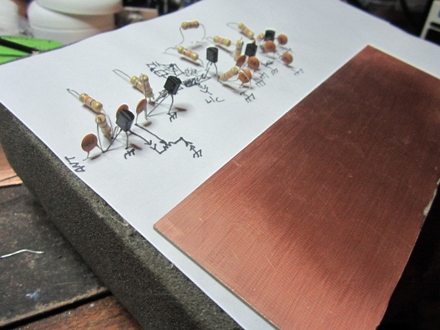 |
| Circuit Layout on Foam |
 | |
| Toy Projector used in layout experiment |
I used this old toy projector that I acquired at a thrift store many years ago, to project the layout directly onto the copper clad.
 | |
| Projecting the layout onto the copper clad |
 |
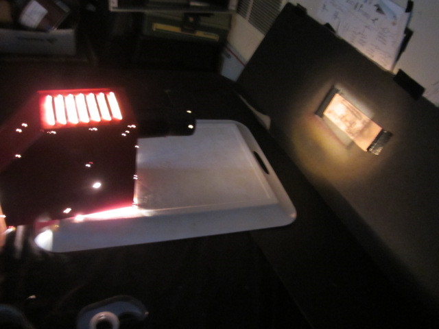
| Safety glasses & a respiratory are mandatory when cutting copper clad! |
Although this method kind of worked, it was a bit of a hassle and didn't turn out as well as I would have liked.
 |
| Result of first layout method experiment. |
Many homebrewers before my time extol the many uses of Blu-Tack, also known as Sticky Tack.
 |
| 'Hombe' Putty Par Excellence |
This is that putty like material that you use in place of thumbtacks to fix a poster to a wall. It can be purchased at just about any department or general store. It was when I was deciding how to build a 40-Meter version of W1FB's Universal VFO from his book, 'W1FB Design Notebook' that I stumbled upon two new uses for Sticky Tack. I am hesitant to say these uses are new, because everything I know about homebrew RF design comes from the grace of those who came before me and openly shared information. However, these two uses are new to me and I hope that they will be new and useful to you as well.
Some authors suggest boiling your toroids after winding them as a way to "anneal" them. Others suggest using Q-dope. I usually use Elmer's wood glue but now I will be using Sticky Tack.from now on. Simply wind your coil around the form. Using your AADE L/C meter (Absolutely essential to successful homebrewing), compress or expand the windings of your coil until the desired inductance is reached. Now place a layer of Sticky Tack on both sides of the coil and join them together around the outside & inside of the coil. Double check that the inductance is correct again and fix it to the desired place on your board. This seems to make the coil quite mechanically stable.
Now on to the second use of Sticky Tack.This was the second layout method experiment that I did. I was much more pleased with the ease of this method and the results in comparison with the projection method.

I start by placing the components on the board by sticking their leads into the putty (StickyTack). Note the coil wrapped in putty to the left side, below the off board variable capacitor.
.jpg)
Ignore the different coil used, not mechanically stabilized in putty, during these layout images.
.jpg)
.jpg)
.jpg)
.jpg)
.jpg)
Once all of your "Putty Pads" are straightened out, use an indelible marker (Sharpie) with a fine tip to trace around each pad.
.jpg)
Remove the putty, and you have your layout. It's still a little less than perfect, but all my circuits are ugly, so I'm fine with that.
.jpg)
I went over the layout one more time with the marker, to make the lines darker and well defined for the next step.
.jpg)
.jpg)
.jpg)
She's a beaut! Cleans up awfully nice doesn't she? Note that the solder already on the board is there because I am reusing this piece of copper clad from an earlier experiment. It is single sided, as it is being used for a VFO.
.jpg)
As always, check for continuity using a multimeter. Make sure all the pads are isolated from each other and ground. If any shorts exist, fix it with a utility knife. (safety glasses!)
----------------------------------------------------------------------------------------------------------
I hope that the above information and images explained this layout method experiment well enough to comprehend. Below are pictures of the build process for the VFO for your enjoyment. It turned out really nicely. :)
.jpg)
.jpg)
.jpg)
.jpg)
.jpg)
.jpg)
.jpg)
.jpg)
.jpg)
.jpg)
.jpg)
.jpg)
So there you have it. I sure would love to hear some feedback. Maybe you have been using this method of layout for a long time. If so, please speak up so we can share suggestions! What uses for Sticky Tack do you find helpful in the RF homebuilding lab?
Thank you for your time. As always, keep your iron hot and stay fluxy!
72,
KE0BFF
FreestateQRP